University of Arizona Tucson, AZ
Description
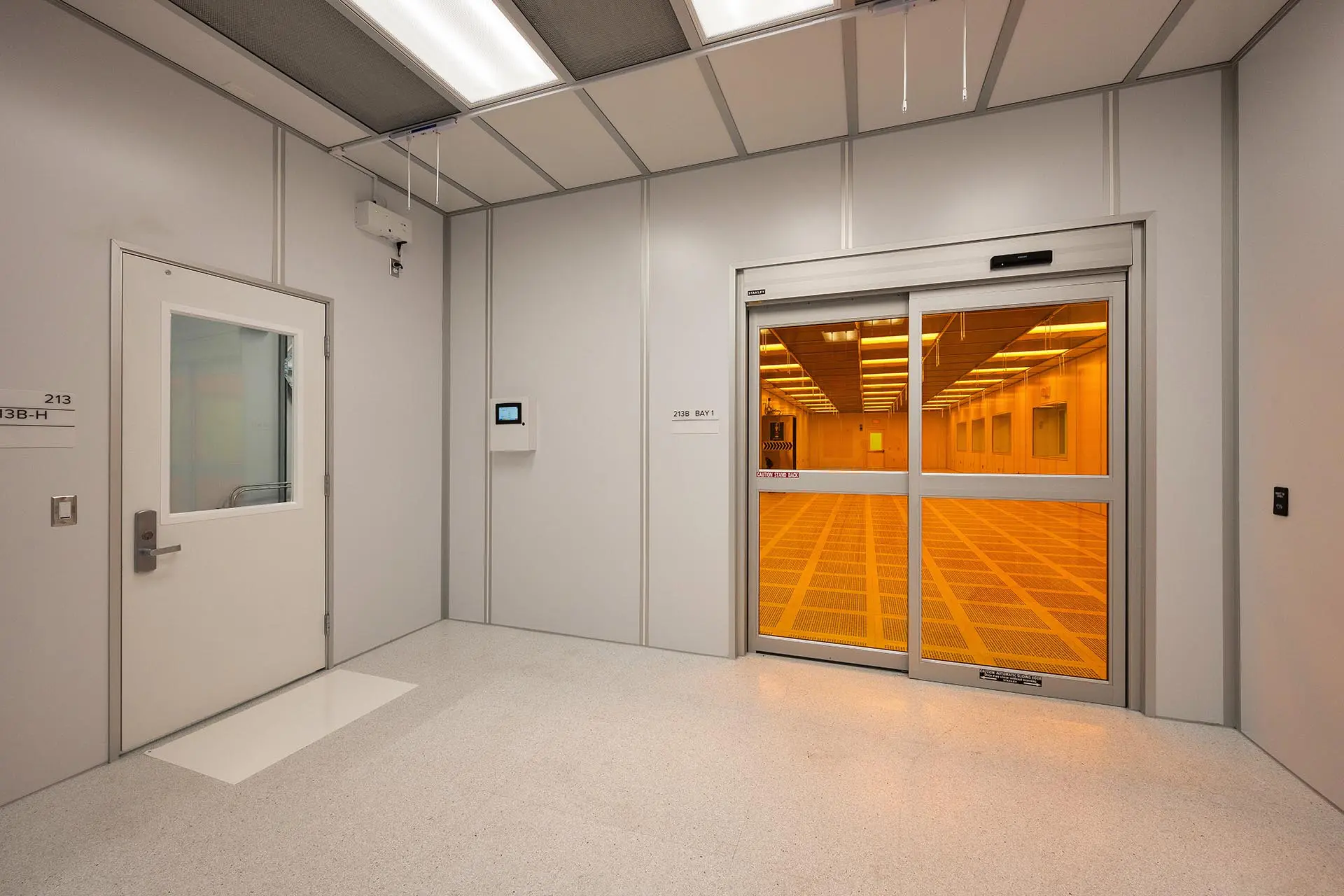
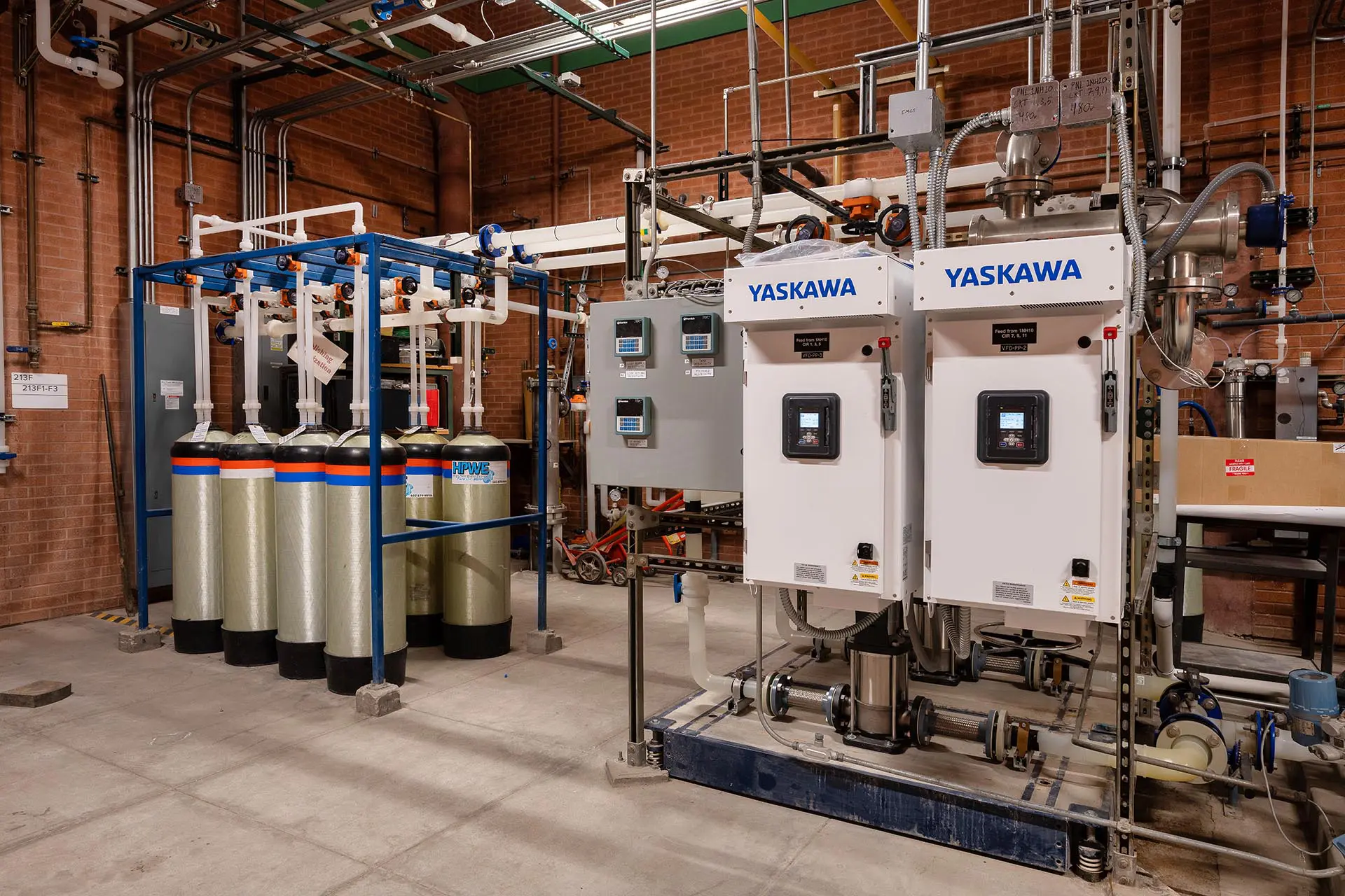
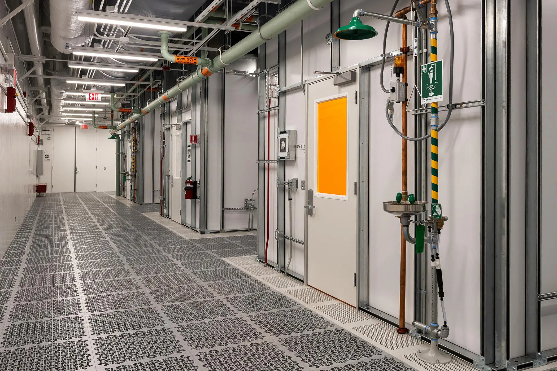
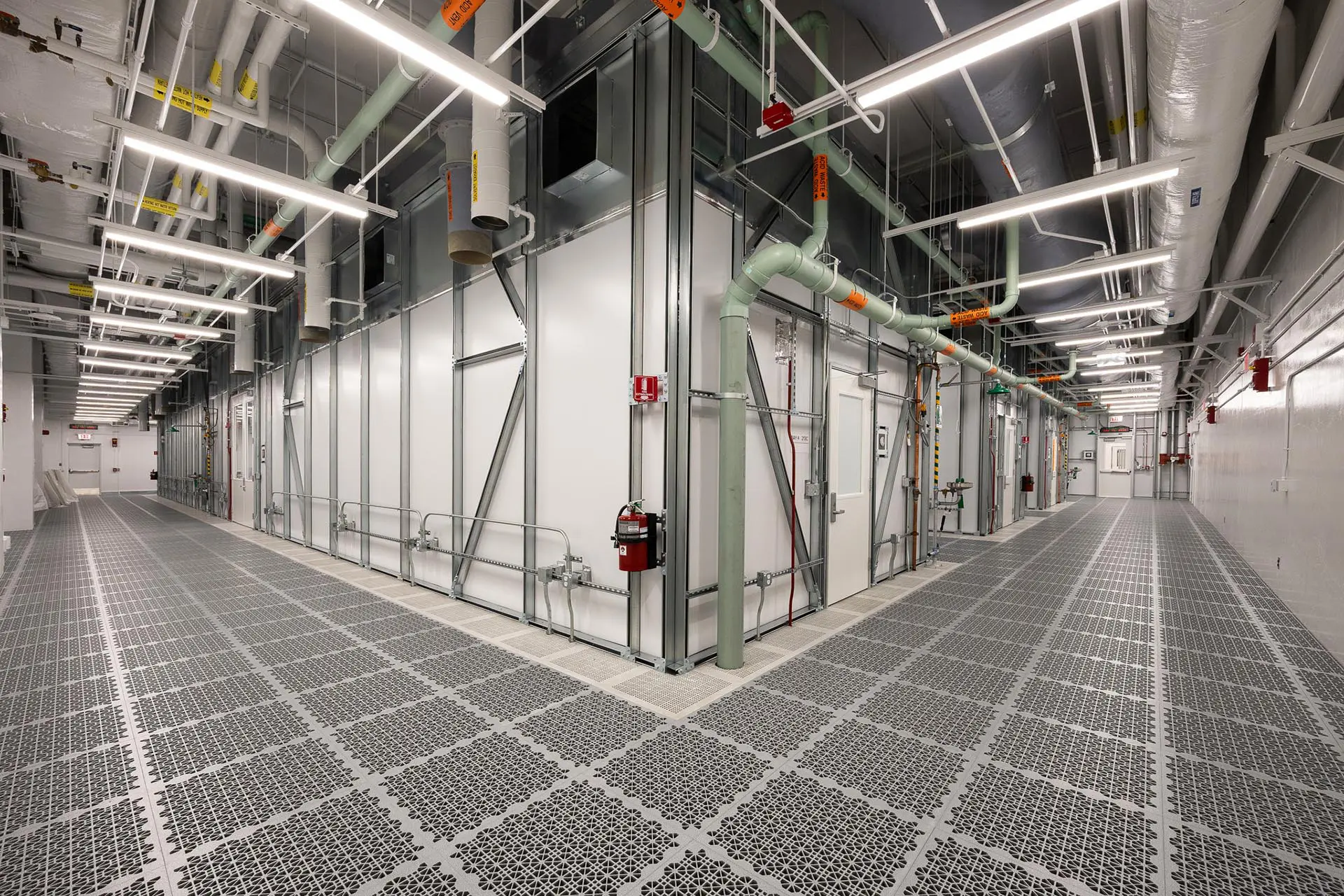
Completed in 2026, Hodess provided design assist services for The University of Arizona Nano Fab Expansion project. Located in the Electrical and Computer Engineering Building, the clean room prepares students for the state’s booming semiconductor industry. It also supports faculty research and industry collaboration on chip fabrication, optoelectronic and photonic devices and quantum technology systems. The ISO 5, 6, and 7 cleanrooms included photolithography, etching, metrology and packaging processes.
Industry
Semiconductor
Project Delivery
Design Build
ISO Class
ISO 5, 6, 7